Affects the distribution of traps in alumina ceramic media. Microstructural analysis shows that different sintering temperatures can lead to different amounts of structural defects in the ceramic media, resulting in different distributions of their traps: ceramics; alumina; trap distribution; sintering temperature. The flashover voltage of insulators in vacuum is lower than that in vacuum. The insulating strength of the vacuum and insulator body is an important factor that restricts the development of high voltage vacuum devices. For example, for high-purity alumina ceramics, which are most commonly used for electrical insulation, its breakdown field strength is as high as 300 to 400 kV/cm. The breakdown field strength is about 350kV/cm, while the flashover voltage of the alumina-vacuum system is generally several tens of kilovolts. In terms of industrial development, the large-scale cutting-edge equipment has huge economic losses due to the occurrence of insulation flashover. In view of the importance of this issue, overseas studies have been conducted since the 1970s. Based on a large number of tests, many studies have been conducted on the flashover of flashover insulator materials in vacuum (Tel 010-62912227- 4228)Li Chengqi (1957-), Male, Professor, Ph.D., Ph.D., mainly engaged in research of high voltage technology and electromagnetic measurement The model, but each model can only explain part of the surface flashover phenomenon in recent years with more in-depth and meticulous research work. Many researchers have proposed a new flashover model based on pitfalls from their own experimental results. However, it is still unclear about the distribution of traps in the medium and how trap distribution affects the flashover characteristics. Isothermal Decay Current was used to investigate the trap distribution of alumina ceramics at different sintering temperatures in order to further reveal The mechanism of flashover provides the basis.
1 Introduction to isothermal decay current method Inevitably, chemical impurities and structural defects are contained in insulating media or semiconductor structures. These impurities and defects result in many energy trapping levels in the bandgap energy gap. These trapping energy levels consist of many localized states that can act as traps or recombination centers. As shown, isothermal decay current method (IDC) is the study of media traps. One of the simple and effective methods for distributing the energy level structure of the conduction band alumina ceramics IDC test requires firstly injecting carriers into the insulating medium under a strong field (electric field or radiation), and carriers of different energy are of different energy levels. Traps trapped; after removing the strong field to get the curve of current change over time The most basic idea of ​​IDC is that current changes with time reflect the release process of carriers at different trap levels; carriers at shallow trap levels are released first After conduction to the conduction band, deep trap levels are released from the carriers 2 Test Method and Step 21 Sample preparation The research object of this thesis is to use the same sintering process, alumina ceramics made at different sintering temperatures, the purity of alumina are It is 99.9%. The shape of the sample is a cylinder with a diameter of 20mm and a thickness of 5mm. The symbol ABC represents the specimens with sintering temperatures of 160C, 1650°C, and 1740C, respectively, and the holding time is 2h. The surface of the specimens was not subjected to ultrasonic cleaning except for any other treatments. 22 Isothermal decay current test The first step was to inject charge into the specimen, as shown in (a). The negative needle-positive plate electrode system is used to inject a charge from the sample with a distance of 1mm from the sample; the test temperature is maintained at 25C. The sample is applied with -11kV DC high voltage, and the voltage is reduced to 0V after pressurizing for 30 minutes. The following procedure records the isothermal decay current-time characteristics: the needle electrode is rapidly removed and a brass column electrode is crimped onto the sample; (The measurement accuracy reaches 1 (116A). Record IDC data is transmitted to the computer through the parallel port 488 cable for carrying out Data Processing 3 Test Results and Discussion 1 Isothermal Decay Current Test Results Test Results The results shown in the figure show that the isothermal decay current I characteristics of the three specimens produced at different sintering temperatures have a huge difference: A has an initial value of 1157 pA. The current value, attenuated nearly 3600 seconds to QB has 120pA initial current value, nearly 3600 seconds decay to C; sample C current is basically 0 isothermal decay current curve also shows that: Sample A releases the most carriers, B times, C is the least.
The trap of alumina ceramic is unipolar injected into the carrier by the electrode. Assuming that the trap is filled, observe the change of the current with time at a constant temperature. The current attenuation reflects the distribution of trap levels Nt(E) Refer to the following formula: The energy density distribution is expressed as Nt(meV)-1(2) to obtain the electron trap energy distribution map, as shown. From the figure, the three samples have almost the same trap center energy level (the energy level corresponding to the peak of the trap distribution), while Sample A has the largest trap density distribution, B times, and C has the smallest trap density distribution. .
3.2 Effect of ceramic microstructure on trap distribution at different sintering temperatures According to ceramic sintering technology, different sintering temperatures affect the microstructure of alumina ceramics. Scanning electron microscopy (SEM) analysis of the samples confirmed the above observations. The SEM topographies of the three samples are shown in the figure. The average grain size of sample A is small (about 3m), the average grain size of sample B is about ym, and the average grain size of sample C is The largest size (about 20m); sample A grain size distribution, sample size distribution of grain size is not uniform; in sample C can be found in the presence of pores according to ceramic sintering technology, ceramic sintering process Actually, the process of reducing the surface energy of the ceramic is higher. The higher the sintering temperature, the better the combination of the original fine crystal grains and the larger crystal grain growth process, so that the grain boundary layer continuously retreats, so that the total grain boundary surface area decreases. The depth and concentration of trap formation are directly related to the crystal growth conditions, crystal structure, and subsequent processing of the crystal sample. The distribution of traps in crystals without impurities is mainly related to crystal structure incompatibility (structure traps).
It is generally believed that the defects mainly exist in the interface between crystal grains and grains, that is, the grain boundary layer is viewed from the SEM image of the sample, probably because the grain boundary unique to the ceramic affects the trap distribution of the medium: the smaller the crystal grains, The more uniform, the larger its grain boundary area becomes, the more traps are contained, and the greater ability to trap charge.
3.3 Effect of surface trap distribution on carrier injection Near the surface of the medium there are a large number of surface states within the forbidden range, ie, trap level solid material at the surface due to the sudden break of the lattice structure, there is an unsaturated bond, It makes the surface very lively and easy to adsorb impurities and gas molecules; the surface grinding, cutting and other operations of the material will also cause many defects on the surface. Under the action of strong field, air ionization and electric field emission can be injected into the surface state from the electrode. Theoretical analysis and experimental results show that the carriers emitted by the electrode are formed in the medium. The space charge is almost concentrated in the medium near the electrode at several microns. From the test results, sample A was injected with more charge, and its surface has the most trap distribution. The distribution of surface traps will inevitably affect the development process of insulator flashover. Further research results will be published in succession. Isothermal decay current method is used. This paper studies the trap distribution characteristics of ceramic insulators prepared at different sintering temperatures. Sintering temperature has a significant impact on the trap distribution of alumina ceramics. Different sintering temperatures mainly affect the trap density distribution of pure alumina ceramic insulators, but have almost no influence on the trap level, ceramic crystals prepared at different sintering temperatures. When the area is the chemical electromotive force that causes the different distribution of the traps, the interference current generated by the insulation of the cable sheath in the detection loop may far exceed the superimposed current, causing the phenomenon of “submergence†when the superposition device and the on-line detection device are in close proximity. Capacitance can be used to block the interference current path. In addition, the compensation electromotive force method can also be used to eliminate the interference current. Currently, on-site detection of XLPE insulation aging has not been recognized as online detection technology and corresponding equipment that can be popularized and applied in the power sector, so the cable insulation aging state Number of There is less accumulation and there is no standard for judging cable aging. Therefore, it is difficult to use the superposition and direct current method to detect the insulation state and remaining life of the cable more accurately. It also requires a long process of accumulating data. Conclusions Online Most of the XLPE cable's insulation status is currently based on the DC method. On the basis of improving the technical level of hardware and software, the DC superposition method will be a practical and feasible method by continuously accumulating data and experience and improving the criteria.
Samsung lm301b Quantum Board 110W
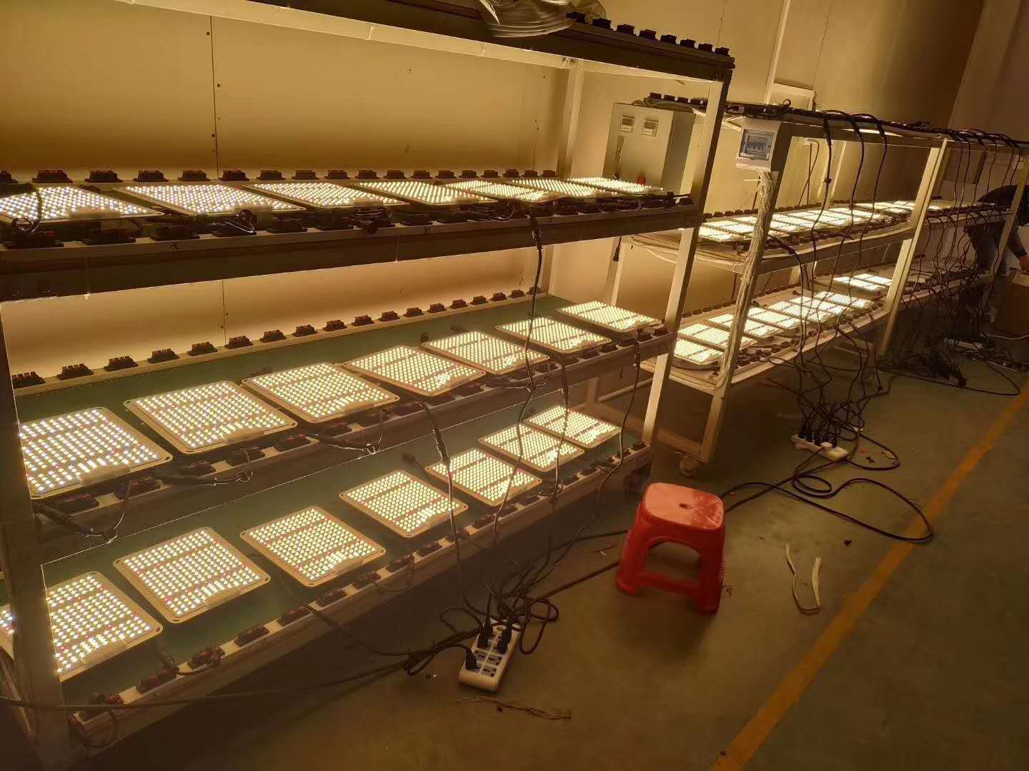
Samsung lm301b Quantum Board 110W, QB350 model, 1board with 350pcs led, meanwell driver, can do knob timer(optional).Can also do spectrum customized. Meanwell driver provide 5 yes warranty, normall driver 1yr warranty.
240W, 450W,600W available too.
System Led Grow Light works both for seeding, veg and bloom stages, promote the plant growth.


Grow Light Quantum Board,Best Quantum Board Grow Light,Diy Quantum Board Grow Light,Samsung Quantum Led Board
Shenzhen Wenyi Lighting Technology Co., Ltd , https://www.wygrows.com