When comparing measurement results with simulation results, the transition from the coaxial cable of the measurement hardware to the signal trace of the device under test is generally considered to be ideal. . Overview When comparing measurement results with simulation results, the transition from the coaxial cable of the measurement hardware to the signal trace of the device under test is generally considered to be ideal. However, in practical applications, this "ideal" state usually leads to data mismatch (simulated data ≠measurement data) at higher frequencies.
 Figure 1: The SMA connector is used to connect the coaxial cable of the measurement hardware to the PCB, convert the coaxial mode signal to the microstrip line mode, and finally to the device under test. Once the analog input/output port is connected to the PCB trace (such as to a microstrip line or coplanar waveguide), this ideal assumption is made by default (Figure 2). While there are many ways to ensure that the transition segment has as little reflection as possible, this particular example highlights the approach to using a complete 3D FEM electromagnetic model for the connector. This approach supports the analytic approach to the parasitic effects of the transition, moving us away from the "ideal" state and becoming more realistic.
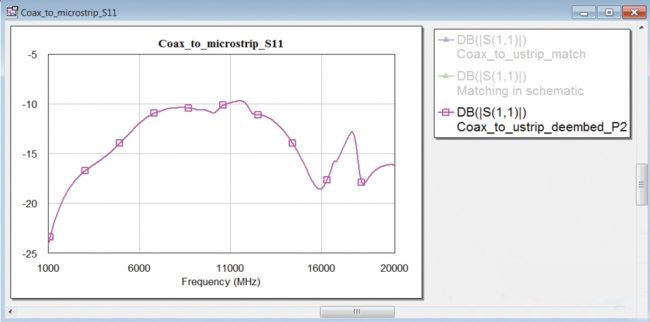
  Figure 2: In general, the emulation port is directly on the microstrip line, ignoring the discontinuity represented by the connector in Figure 1, and thus systematically distorting the simulation results and measurement results. Design In the schematic (parent documentation), we have drawn a printed circuit board (PCB) with signal traces. The 3D connector designed for a 20 mil substrate is technically a sub-model (or sub-model) of the parent document, which means that the design is layered. The connector model allows one port (input port) to be placed at the end of the connector's coaxial cable, and the other ports are defined as ordinary wave ports (output ports) at the end of the microstrip line. The reference plane of the output port is moved to the back of the connector. Unoptimized Transfer Quality The transfer curve S11 in Figure 3 shows that a good intrinsic match is only about 2 GHz. At the target design frequency of 10 GHz, the reflection is as high as -10 dB. Clearly, the design will now benefit from optimized switching, not only because of the lost energy, but also because mismatch is an important source of measurement and simulation bias.
Figure 3: Conversion segment reflection coefficient at the coaxial port before optimization. Optimization Strategy The transfer model can be optimized using the electromagnetic document as a normal submodel in the schematic. It is easy to determine that the matching circuit of series L and parallel C can complete the optimization of 10 GHz. In the microstrip line, the series L can be realized with a narrow strip line segment, and the parallel C can be realized with a wide strip line segment. Therefore, optimizing the required microstrip size is very simple, as shown in Figure 4.
 Figure 4: Candidate matching circuit that can be used to optimize the transition from coaxial to microstrip line. The final step is to put the matching circuit size into the 3D model and then perform the verification simulation, as shown in Figure 6.
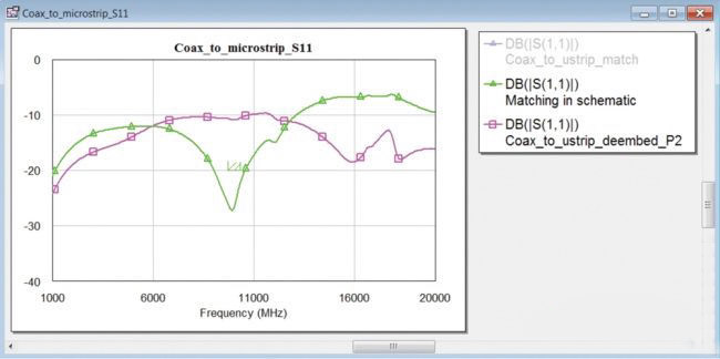
Figure 5: Transfer segment reflection coefficient (green curve) when a closed model of the matching circuit is used on the coaxial port.
 Figure 6: Surface current annotation for an optimized segment at 10 GHz. As can be seen from the figure, the first matching test is very good. It is also beneficial to observe and animate the surface current at 10 GHz, as shown in Figure 7.
  Figure 7: Surface current annotation for an optimized segment at 10 GHz. In summary, this simple matching circuit allows signal transmission from the coaxial cable to the microstrip line to have less than -20 dB of reflection performance at the 10 GHz target design frequency. The matching bandwidth is approximately 2 GHz and it is convenient and reliable to optimize using traditional circuit models with connector electromagnetic models. The complete 3D electromagnetic verification solution is available immediately and the geometry is optimized.
 The various transfer models from different connectors to different circuit substrates can be stored as a library and then conveniently recalled in any subsequent circuit design. The integrated 3D electromagnetic tool supports keeping all design data in an AWR Design Environment (AWRDE) project file, including connectors, bound packages, enclosures, or any other arbitrary 3D object. This eliminates the risk of misuse of the model, for example: the horizontal connector is changed to a vertical connector; the graphical view of the design layout will immediately show which 3D model is being used, which evaluates the S-parameters of the connector elsewhere And then importing AWRDE as a blind file is different. Single project files also mean easier archiving, design delivery, storage, and reuse.
Http://?itemid=452
Http://news.chinawj.com.cn
 Editor: (Hardware Business Network Information Center) http://news.chinawj.com.cn
Electric Heated Towel Rack,Towel Heater, Heated Towel Bar, Wall Mounted Towel Warmer
Jiangmen Faer Sanitary Co.,Ltd , https://www.faersanitarys.com